William Love Receives First Place Texas Insturments Prize for Best NanoJapan Research Poster Presentation
William Love received the first place Texas Instrument Prize for the Best NanoJapan Poster Presentation award at the 2009 Rice Quantum Institute Summer Research Colloquium for his poster presentation on Half-Metallic Heusler Alloy Based Magnetic Tunnel Junctions.
Why NanoJapan?
The NanoJapan program allows aspiring students in engineering and physics to conduct research in active scientific fields. This allows the students to see the practical application of classroom topics and how they are being used in modern scientific research. In addition, the program exposes students to another culture and teaches these students how to work as part of a team. I chose to apply to the NanoJapan program because it is an excellent opportunity to gain top level research experience in physics as well as exposing me to another culture. I have been interested in Japan through my studies in Karate and I had always wanted to visit Japan, so the NanoJapan program is a perfect synergy of my love of physics and Japan. I believe that the program will be a great asset to my undergraduate education since it will provide a connection from the basic principles of physics that I have learned through classes to how these principles are being applied in actual scientific research. The program will also teach me how to work in a laboratory which is knowledge I will use when I eventually conduct research at my home university. I am looking forward to being immersed in the Japanese culture and living in a foreign country. I am also eager to learn about nanotechnology and work in an actual scientific laboratory; which is something that I have wanted to do ever since I was young. Overall, I am very excited about working in Japan and gaining knowledge and experiences that I know will be with me forever.
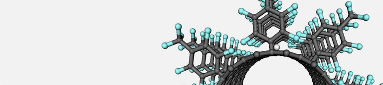
Research Project Overview - "Half-Metallic Heusler Alloy Based Magnetic Tunnel Junctions" ![]()
My research involved fabricating and testing Co2MnGe based magnetic tunnel junctions (MTJs). More specifically, we were testing the effect of changing the manganese composition and how that changed the tunnel magneto resistance (TMR) ratio at 4.2 Kelvin. We fabricated the devices using a Molecular Beam Epitaxy machine and fabricated them using photolithography and argon ion milling. We then bonded the MTJ to a DIP chip and connected the electrodes of the MTJ to the DIP chip. We then measured the TMR ratio at 4.2 K.
My research is related to both quantum physics and solid state physics, which are both fields that I am considering to follow into graduate school. While I do not know if I will work on any similar research in the future, the experience of being in an international laboratory was invaluable. I can also now see that conducting scientific research makes you not only part of a national scientific community, but also a global scientific community. After seeing my Japanese lab mates give presentation about their research all over the world, I now have more of a global view to scientific research and can see how everything fits together in the big picture.
Daily Life in Japan
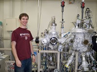
Yamamoto-sensei’s lab is a fairly typical Japanese laboratory. Most of the members of the lab are Japanese so Japanese is the language that is spoken normally in daily conversation. All of the lab members know some English and typically the higher the person's education level the more English they know. All of the sensei’s in the lab are fluent in English and the post-docs are almost fluent. For the first few weeks in the lab I was shown how to operate the equipment by various different lab members but once I started working on my research project I worked almost exclusively with my mentor, Taira-san. I did the research myself but Taira-san was always there in case something went wrong or if I had any questions. Since I didn’t know a lot about the physics behind the research, Yamamoto-sensei gave me and some of the other undergraduate students in the laboratory lectures about the basics behind the research.
Every day I would wake up around 7:00 am, have breakfast in my room, and then leave around 8:40 to bike to Hokkaido University. The dorm that I lived in was about a 30 minute walk or 15 minute bike ride to my lab on campus. I would then do various things in my lab till about 1:00 and then I would have lunch with my lab mates in one of the student cafeterias on campus. I would normally leave the lab around 6:00 but I sometimes stayed as late as 9:00 or 10:00. For dinner I would normally eat some food in my room that I bought at a local grocery store or eat out with the other NanoJapan students. The dorm that I lived in had a shared kitchen with microwaves and stoves but I never made anything more ambitious than sandwiches. On the weekends, I would normally go see some local places around Sapporo or go on longer trips around Hokkaido with Claire and Erin.
 |
 |
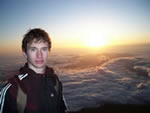
On top of Mt. Fuji |
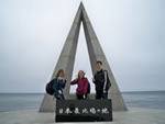
Cape Soya in N. Hokkaido |
My Favorite Experience in Japan was...
Either climbing Mt. Fuji with the other NanoJapan students or traveling to northern Hokkaido and going to Rebun and Rishiri Island.
Before I left for Japan I wish I had...
Learned katakana and hiragana. The language classes move too quickly to spend time teaching us these alphabets and they are incredibly useful to know from when you first arrive. Try to memorize them before you go.
While I was in Japan I wish I had...
Taken formal Japanese classes at Hokkaido University. It would have been nice to learn a little more Japanese in a setting where I could apply it on a daily basis.
Tips for Future NanoJapan Participants
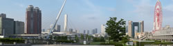
Odaiba, Tokyo
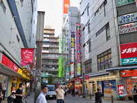
Akihabara, Tokyo